L.M.A.Means
 Deposition
Systems
Deposition
Systems
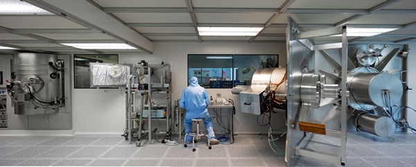
 Ion Beam Sputtering
system installed in a ISO3 clean room (size
2,4*2,4*2,2 m)- (c) Cyril Fresillon Photothèque CNRS
Ion Beam Sputtering
system installed in a ISO3 clean room (size
2,4*2,4*2,2 m)- (c) Cyril Fresillon Photothèque CNRS
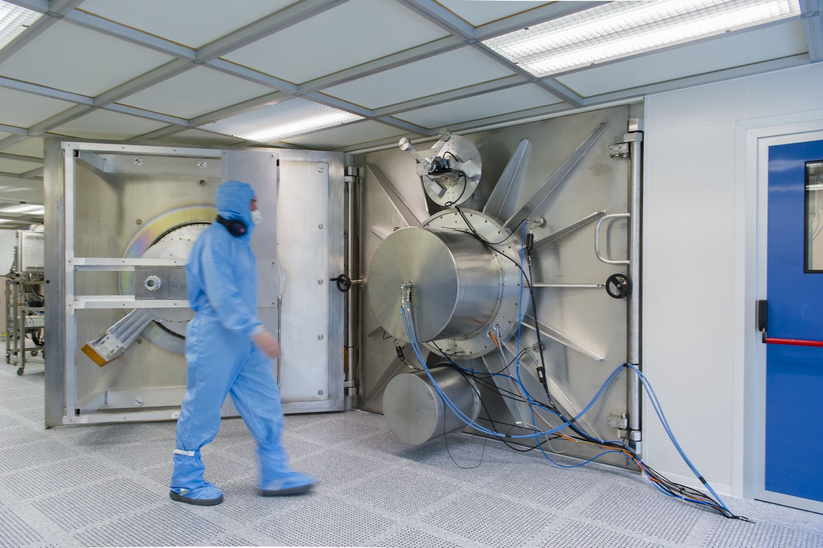

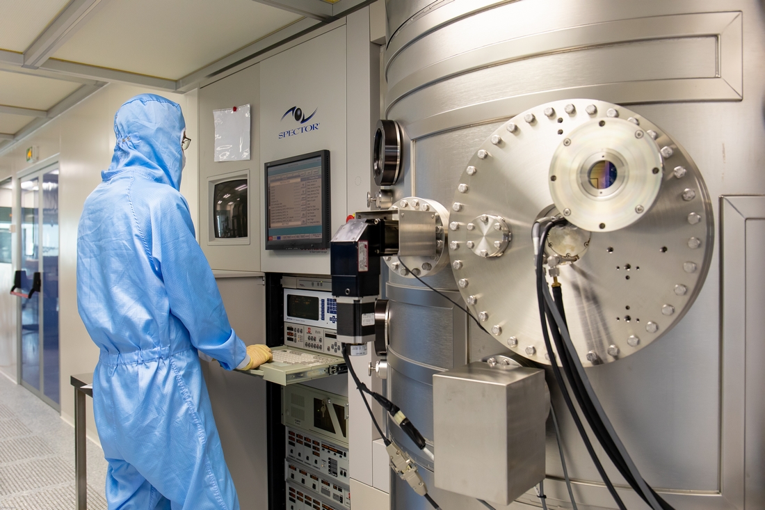
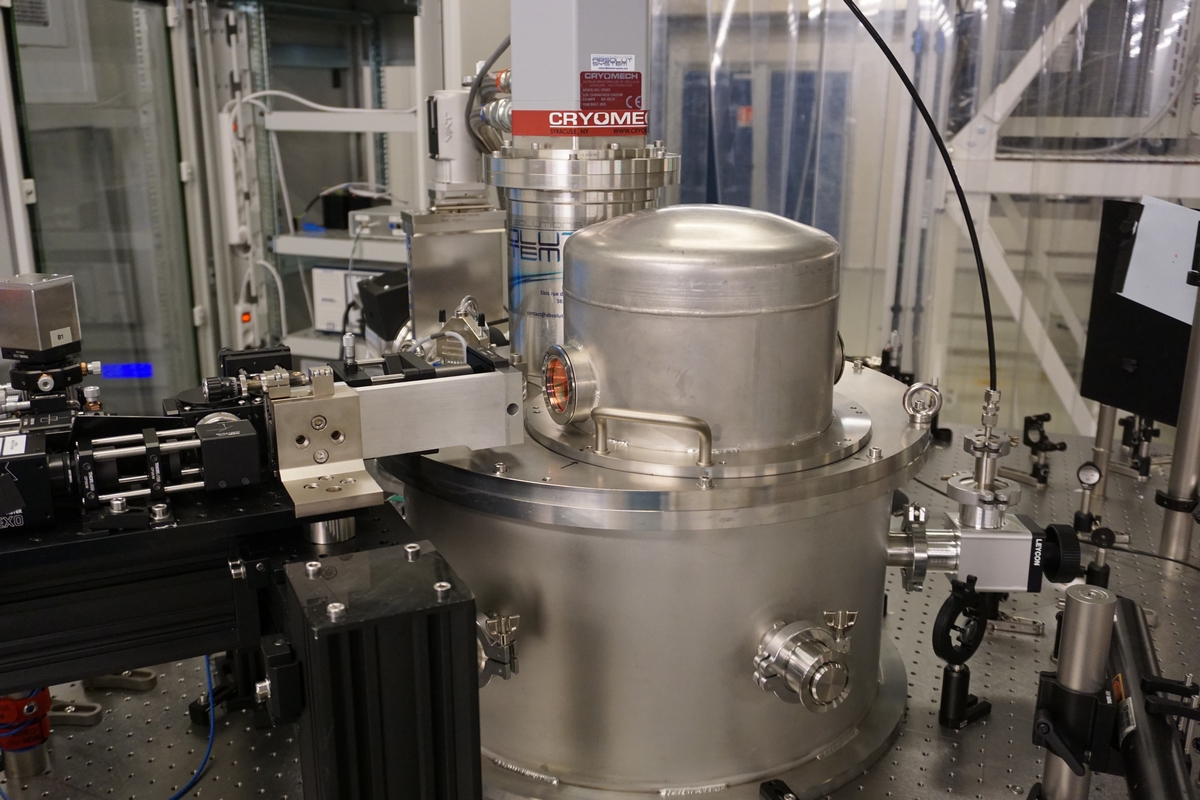
- Dual Ion Beam Sputtering
system installed in a ISO3 clean room : model SPECTOR from IonTech (Veeco) (size:
diameter 1.1 m, height 0.9 m) - (c) Cyril Fresillon Photothèque CNRS
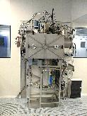
- Dual Ion Beam Sputtering
system installed in a ISO 3 clean room (size
0,6*0,6*0,8 m)
- Ion Assisted Deposition system (VPTECH Citation 54") installed in a ISO 5
clean room - (c) Cyril Fresillon Photothèque CNRS

Optical and Mechanical Characterizations
- Absorption PDS (Photothermal Deflection System) benches at 1064 nm and 1,5 µm - Mapping possible up
to 30 cm in diameter - Surface and volume measurement
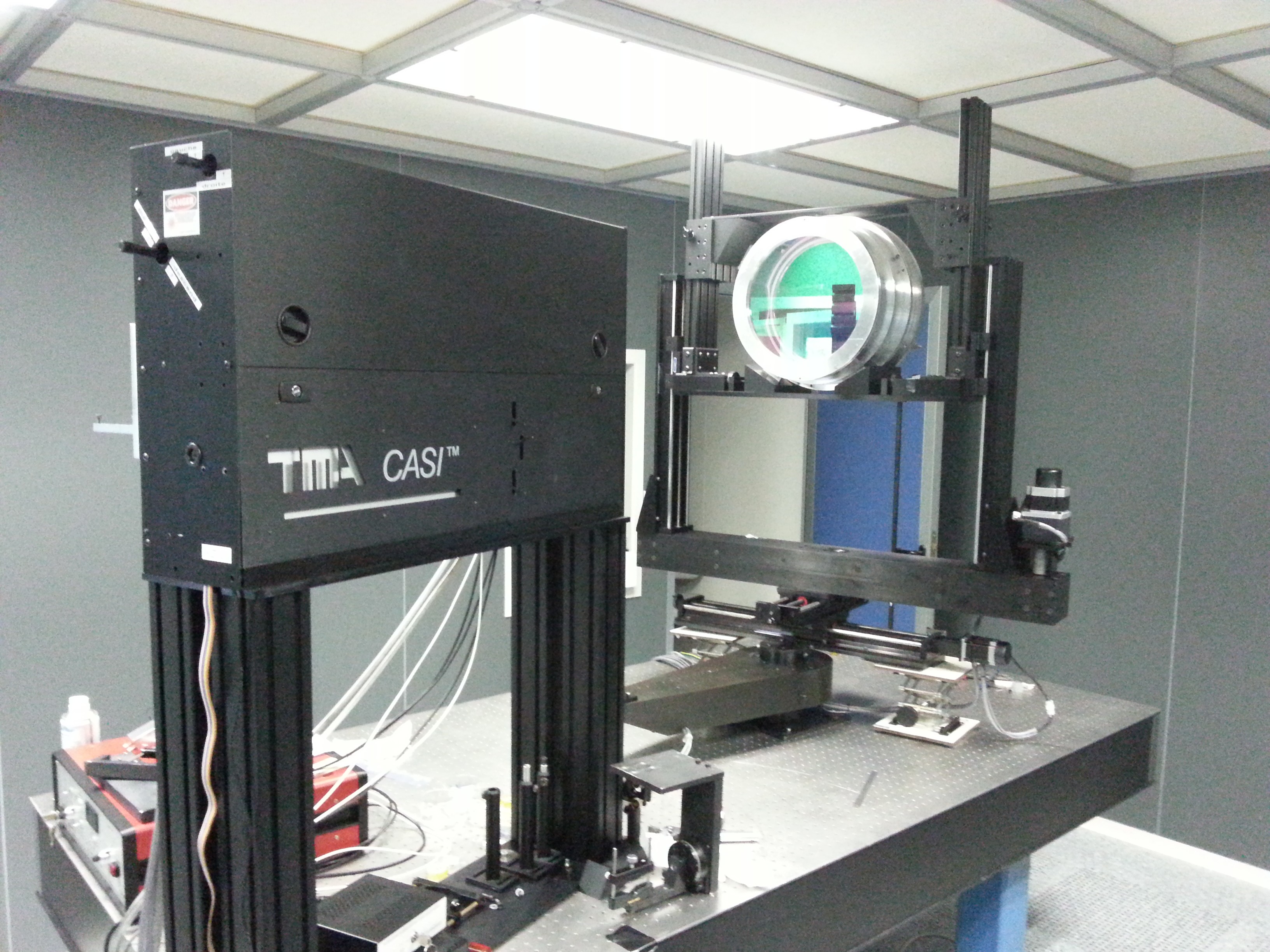
- Scatterometer
CASI (ScatterWorks, ex TMA) at 633 nm, 1064 nm - Mapping possible on 40 cm in diameter
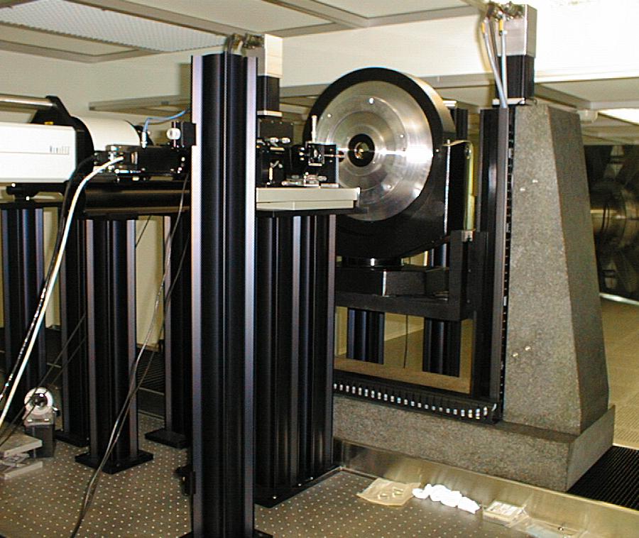
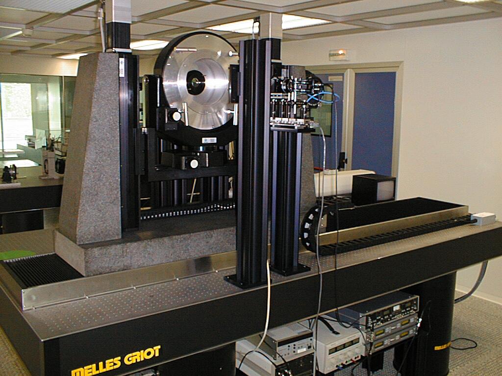
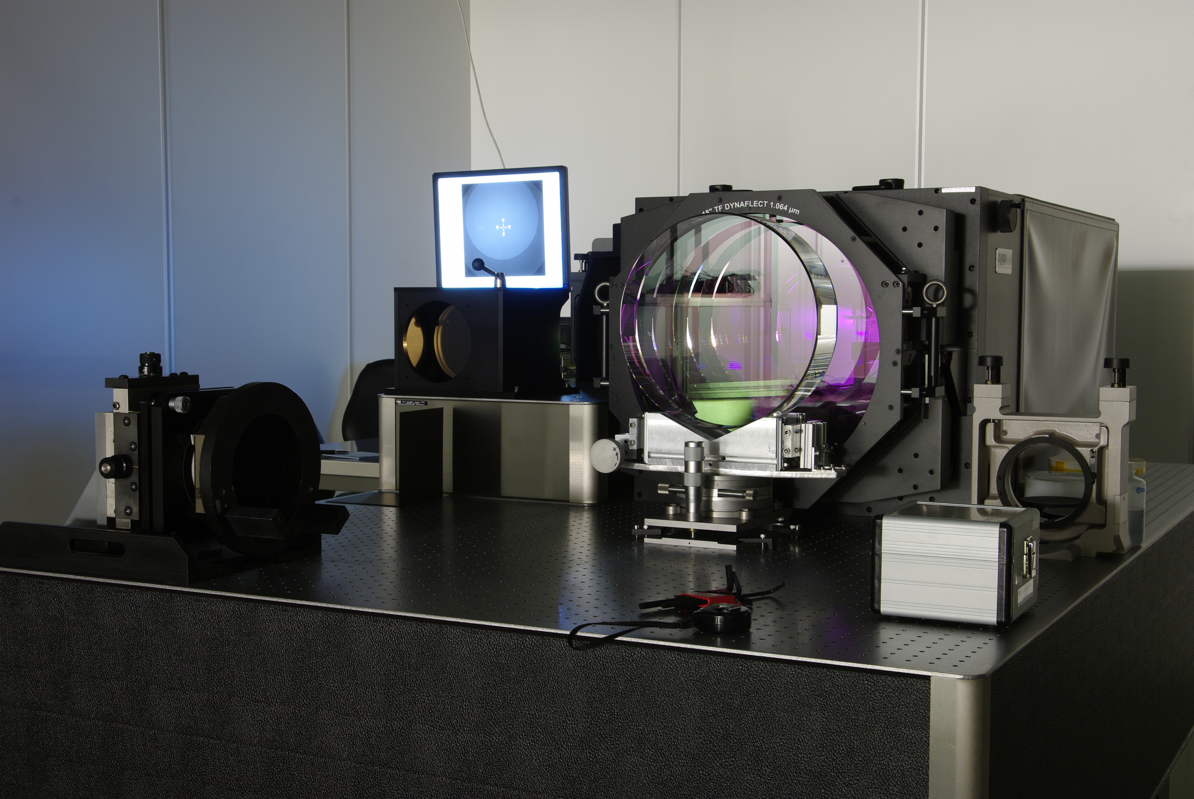
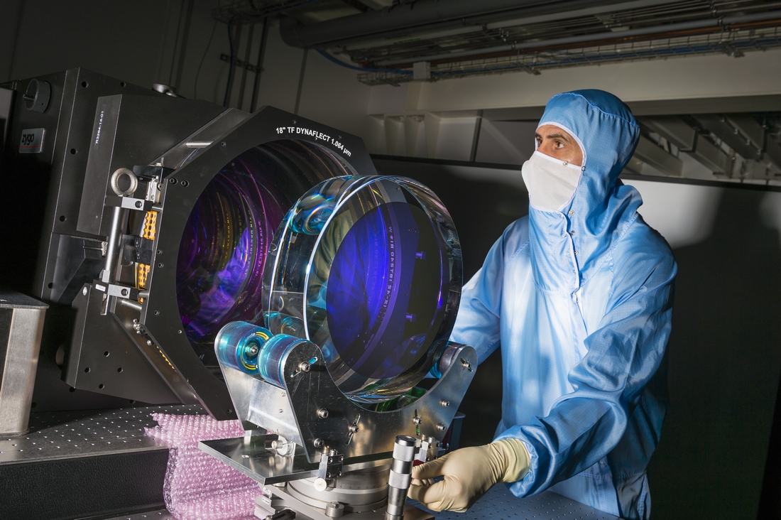
- ZYGO wavelength shifting
interferometer (VERIFIRE) with a 18" beam expander (1064 nm), pupil diameter 450 mm: measurement of surface flatness below 0.5 nm RMS
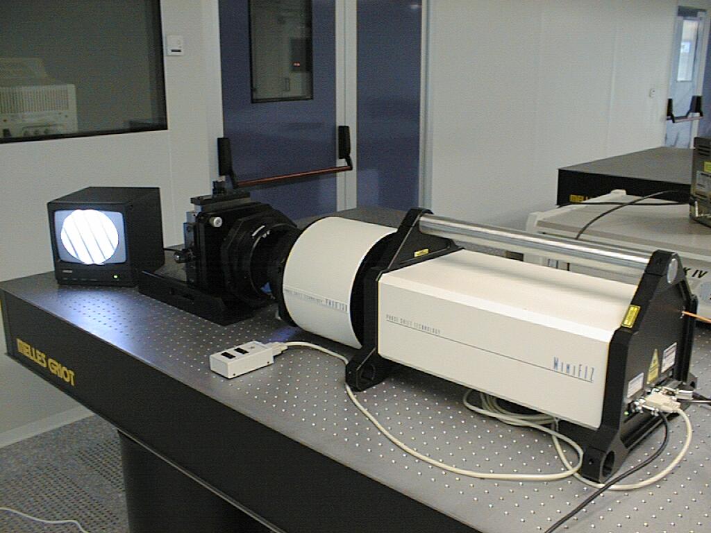
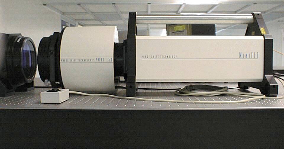
- Phase
Shift interferometer model MINIFIZ(1064 nm), pupil diameter 150 mm
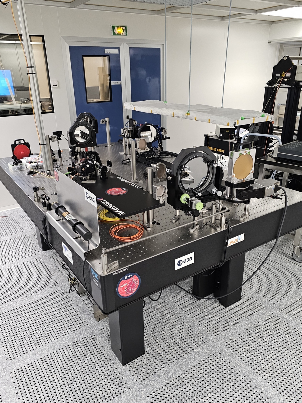
- OBSERVE bench(ESA) to measure the
wavefront error of mirrors every nm from 510 to 950 nm, with variable incidence and variable polarization - Bench developed
by the company IMAGINE OPTIQUE and installed at the LMA in the ISO3 clean room (bench developed to measure the Dichroic of the EUCLID satellite)
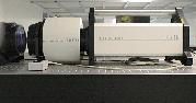
- UV-Visible-Near
IR spectrophotometer Lambda 1050 PERKIN-ELMER (3200-200 nm), three detectors available, URA accessory (Absolute reflectivity
measurement available)
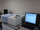
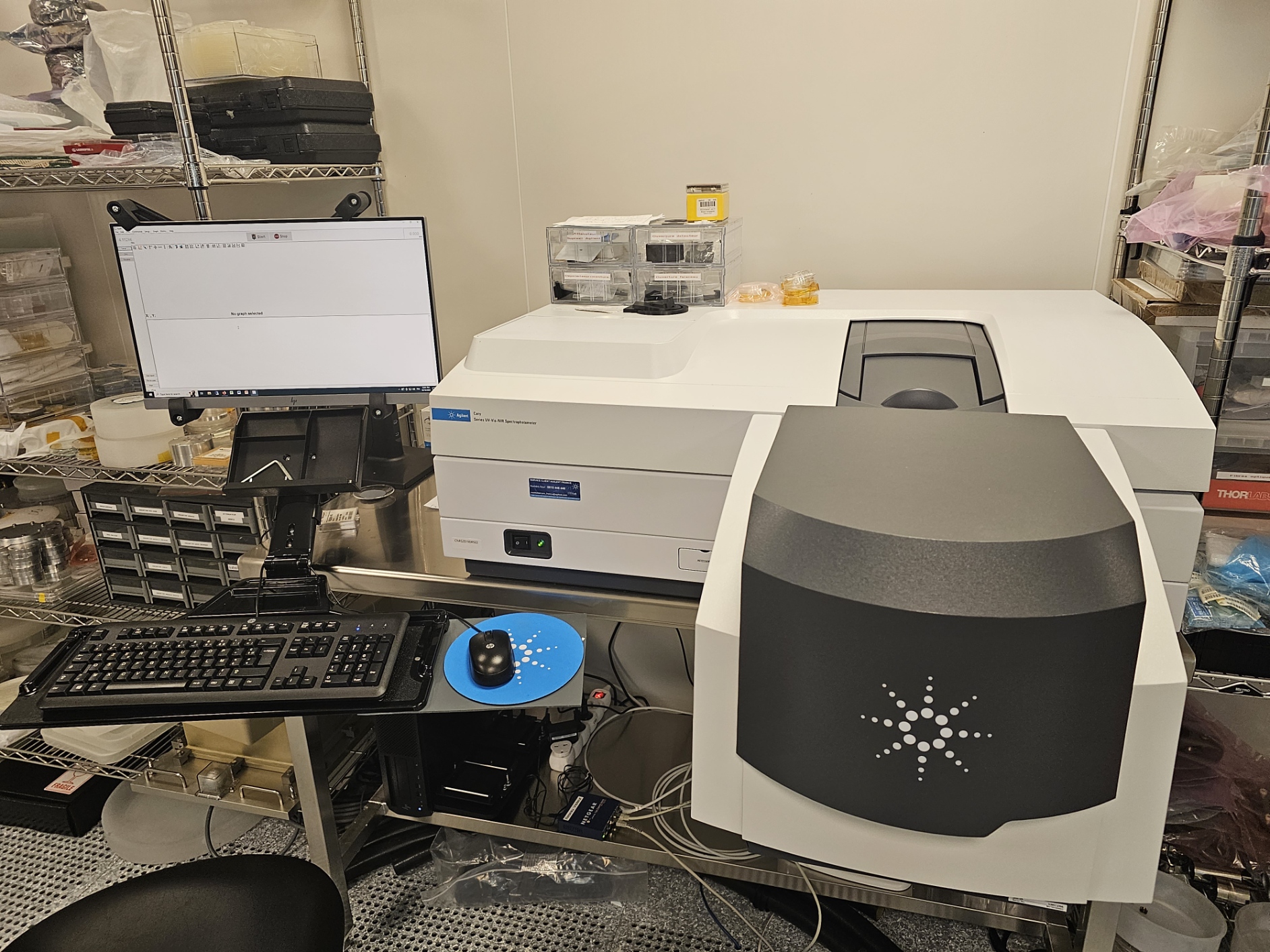
- spectrophotometer
UV-Visible-Proche IR CARY 7000 Universal Measurement Spectrophotometer (UMS) AGILENT (3300-175 nm),
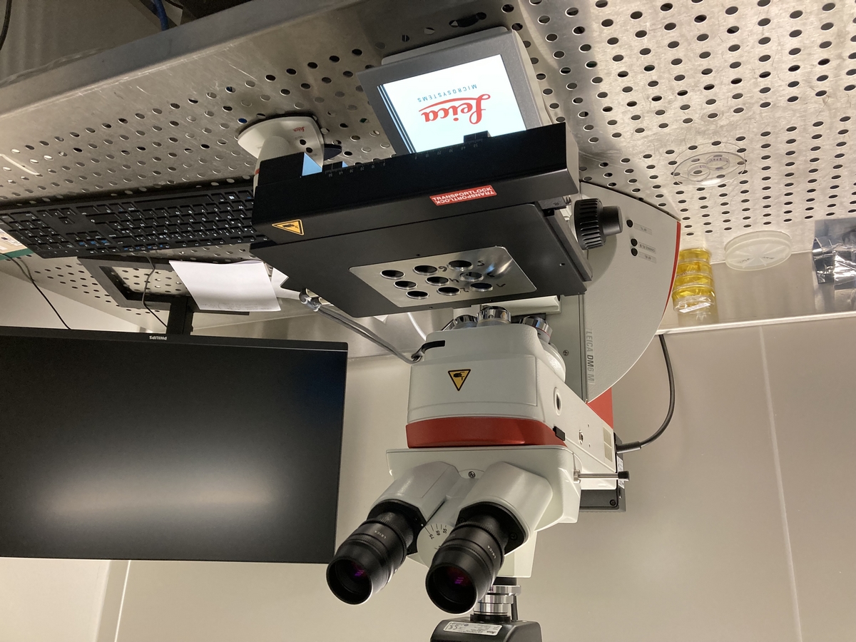
- Microscope optique Leica Leica DM6/M optical microscope, able to measure defects up
to a size of 5 µm, automatic scanning of surfaces.
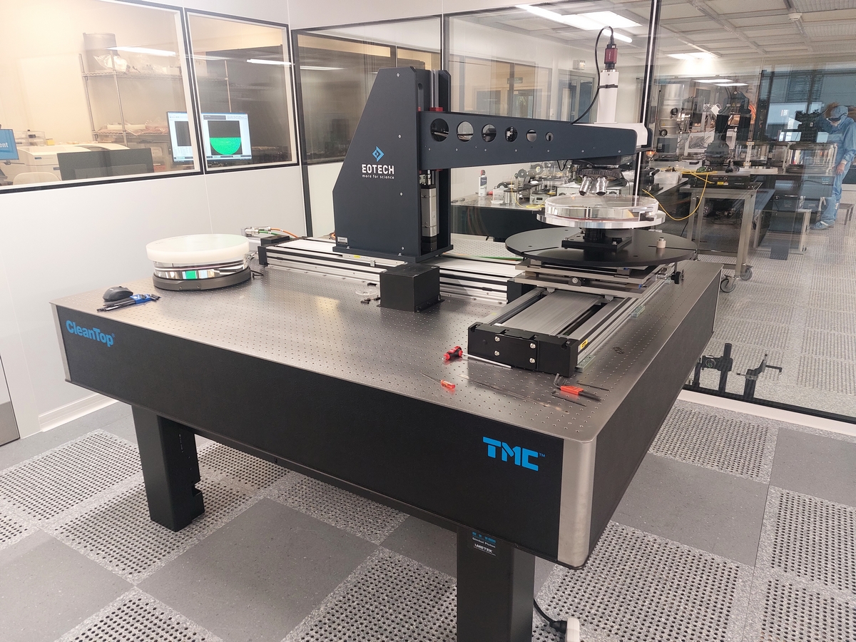
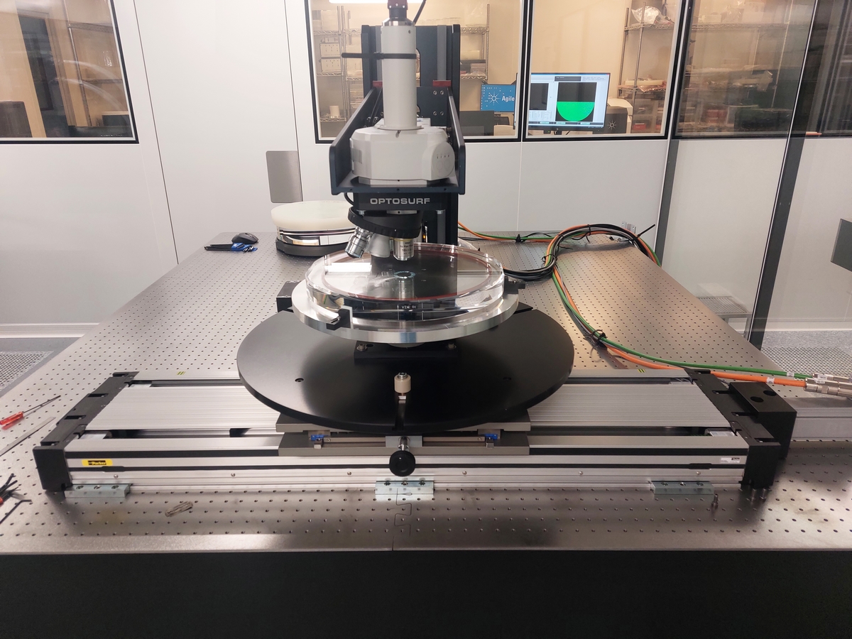
- Optical profilometer
EOTECH - Microroughness measurement, Defects maps of 500*500 mm
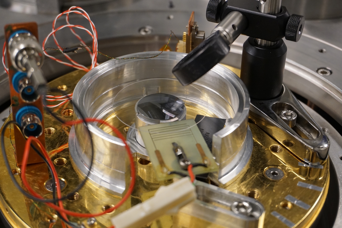
- Three benches to measure the mechanical Quality factor Q (mechanical loss angle) based
on the GeNS (Gentle Nodal Suspension) technique, measurements at room temperature and cryogenic temperature
- Simulation program
ot thin films (calcul and optimization of any type of multilayers with OPTILAYER and TFCALC)